NovaCentrix provides next-generation, smart packaging processing tools and conductive inks for sensors, displays, and energy storage.
NovaCentrix’s PulseForge® photonic curing tools are used for drying and sintering high-temperature, high-performance electrically conductive inks directly on paper and plastic films at high-production rates.
The company’s Metalon® and PChem silver and copper inks offer exceptional conductive performance at industry-leading pricing, with a team of experts ready to answer any product questions, for prototyping concepts, and for working with client product teams.
NovaCentrix’s products are already used in production printed electronics applications.
Photonic curing tools for drying and sintering electrically conductive inks
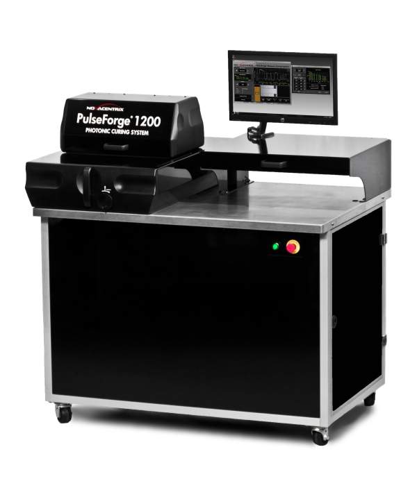
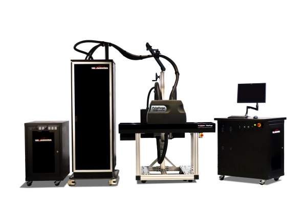
PulseForge photonic curing tools from NovaCentrix are state-of-the-art conductive inks processors.
Photonic curing is a patented materials processing method developed by NovaCentrix and refined over a decade for printed electronics applications.
The photonic curing tool uses high-speed, high-power flash-lamps to heat conductive inks and films with millisecond pulses to very-high temperatures without damaging underlying or adjacent materials like paper or plastics.
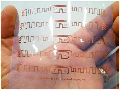
Through adjustment of the flash-lamp pulse settings, the PulseForge tools can dry and sinter inkjet prints only a few tens-of-nanometres thick, all the way to screen-printed layers more than 50µ thick. This allows conventional and new low-cost conductive inks to be used in applications that were previously not possible or economically viable.
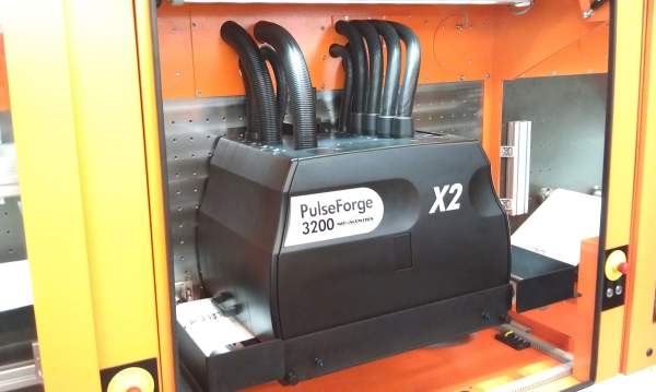
Photonic curing is ideal for use in high-speed print lines as the tools can be placed in-line with printer stations. PulseForge tools can augment or replace other thermal processing such as dryers and only require a few feet of in-line space for retro-fitting to existing production systems.
Advanced, functional and economical thermal printing process
Customers use the PulseForge photonic curing tools for a variety of reasons. For some, the use of the tools allows them to add functional printing economically to their existing print capabilities, which can open new markets and allow customers to seek higher-value projects.
For others, the use of the PulseForge tools allows them to build innovative products that are not possible using traditional thermal process methods. These products typically require additional investments in R&D development and NovaCentrix provides expertise for these efforts.
PulseForge also significantly increases production rates and prevents the need to add additional space-consuming dryers.
High-performance electrically conductive silver, copper, carbon and nickel inks
NovaCentrix has also developed the Metalon and PChem high-performance electrically-conductive inks, available with silver, copper, carbon, nickel and other materials.
Metalon and PChem inks are water-based so release minimal volatile organic compounds (VOC) when being cured.
The Metalon ICI ink prints as copper oxide, which is then converted to copper with the PulseForge tools. This ink is only $75/kg in production volumes.
Formulations can be selected based on the type of substrate, the type of conductivity needed and the type of deposition to be used. NovaCentrix also develops custom formulations. Formulation can be selected for use with traditional thermal processes, while others, which are optimised for processing using the PulseForge photonic curing tools, can be selected.
Pilot and manufacturing-scale inkjet, flexographic and screen printing services
NovaCentrix offers contract services at its 40,000ft² facility in Austin, Texas, US, for pilot and manufacturing-scale production of printed electronics, from quantities of a single unit to 100 million units.
The company’s print capabilities include inkjet, flexographic and screen printing, while it can also accommodate sheet or roll-based operations. NovaCentrix can manufacture conductive patterns, which can then be integrated into packaging solutions.
Optimising smart packaging systems
NovaCentrix’s team is available to work together with customers in developing and optimising smart packaging systems. The company is happy to do the heavy-lifting for system design and to provide education for its customers in printed electronics technologies, which are important for customers’ businesses.
Contact the company for more information. NovaCentrix is ready to work with you, whether it is reviewing current capabilities related to printed electronics or development on a specific product or project.
Feel free to coordinate with NovaCentrix to visit its facility in Texas, where it can demonstrate its capabilities and discuss how they can help your business or projects.


